Company Details

Yuheng Optics Co., Ltd.(Changchun)
Company Details
Yuheng Optics Co., Ltd.(Changchun)


The figure is an absolute value circuit, that is, a circuit that converts AC to DC. Among them, as shown in Figure (a) is the most basic absolute value circuit, which is composed of a negative ideal diode circuit and an addition circuit, and outputs U. Equal to the two half cycles of Ui, if the capacitor C1 is connected to the inverting input and output of A2, the Bellow output is smooth DC. The relationship between the resistance values should be R1=R2, R5=2R4, and Av=R6R5. Figure (b) shows the circuit with high input impedance. The working principle of the circuit is as follows: when the input voltage is positive half cycle, VD1 is turned on, A1 is working as follower state; when negative half cycle is turned on, VD2 is turned on as shown in (c) is an absolute value circuit in which all resistors are equal. In the positive half cycle, =U1=Ui, VD2 is not conducting, and U is output. =-(-Ui×(R5/R4))=+Ui. VD1 is not conducting during the negative half cycle, +U2=-Ui[(R3+R4)R2]/Ri. If R1 to R5 are equal, +U2=-1/3Ui, so U. =-Ui(2/3+1/3)=-Ui. Figure (d) is an absolute value basic amplifying circuit using an ideal diode. The A1 and A2 use the high-speed op amps LM318 and HA2525. Figure (e) is an example of an absolute value high speed amplifying circuit. In the circuit, the constant current source composed of VT and VT2 and the voltage drop on RB1 and RB2 are biased to A1, and the circuit configuration is simple, and the frequency characteristic of the absolute value amplifier can be several hundred kHz or more. Figure (f) is an absolute value circuit composed of an analog switch and a zero-crossing comparator. In the circuit, the inverting input of A1 is connected to the non-inverting input terminal, and the potentials are equal. When the analog switch DG201 is turned on, that is, the input signal is positive half cycle, A2 outputs a high level, which is the follower working state. A2 outputs a low level during the negative half cycle, which is the inverter operating state. The response characteristics of A2 and DG201 are the highest operating frequencies, and their operating frequencies range from low frequencies to 10 kHz. As shown in Figure (g), the standard DC converts the input AC power of 1V to 10V DC. The circuit is an absolute value circuit using an ideal diode. The input and output are linear and the signal range used is very wide. The RP is used to adjust the gain and C1 is the smoothing capacitor. Figure (h) is also a standard DC conversion circuit, but the rectification method is different. Two smoothing capacitors, C1 and C2, are used. 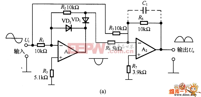 (a) the most basic absolute value circuit
 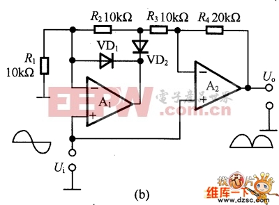 (b) High input impedance circuit
 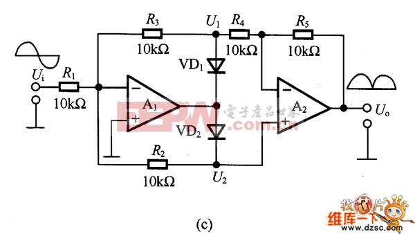 (c) Absolute value circuits with equal resistance
 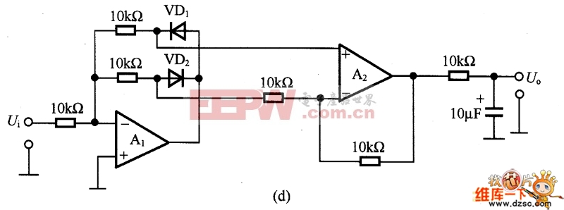 (d) Absolute value basic amplifying circuit using ideal diode
 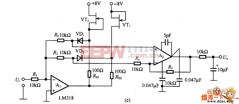 (e) Absolute value high speed amplifier circuit
 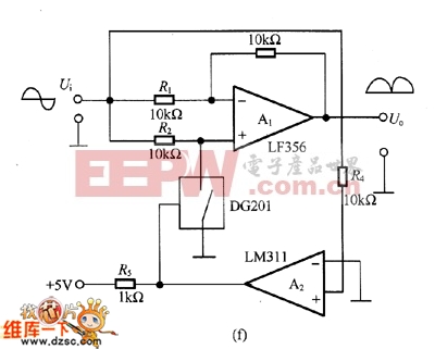 (f) Absolute value circuit composed of analog switch and zero-crossing comparator
 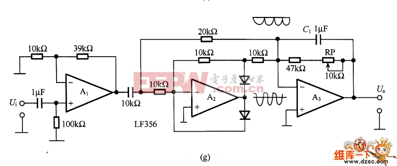 (g) One of the standard DC conversion circuits
 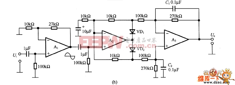 (h) The standard DC conversion circuit is shown as the absolute value circuit